Single stepping an ATmega with a FPGA
As continuation of the post about the internals of the clock of an ATMega, I decided to test the possibilities of simulating a clock using a FPGA, in particular using my loyal mojo development board.
My intent is to create a system to generate glitching with an external clock, but since I like to proceed one step at times I start creating a 16MHz clock that can be switched to a manual pulse to create a single step atmega.
The process included the use of a FPGA, a minimal circuit with a microcontroller
and some C code.
All can be summarised with the following (fantastic) hand drawn diagram
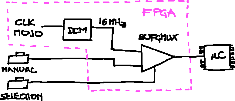
FPGA
The FPGA is used to create and manage the clock and then to output it to an external pin of a microcontroller. This operation of getting a clock in an output pin is called clock forwarding.
The spartan-6 has special internal network for lines that handle clock signals, it's called clock network: it provides a low capacitance, low skew interconnect lines that are well suited to carrying high frequencies. All you want to know about clock for the Spartan-6 is documented into the Spartan-6 FPGA Clocking Resources
In our experiment we need to create the clock, route it into the clock network and then output it from an external pin.
DCM
First of all we need to generate a 16MHz clock; in a Spartan-6 FPGA we have available the DCM_SP primitive,
DCM stands for Digital Clock Management, it's a building block available into the FPGA
to manage clock related signals. Internally it uses a Phase Locked Loop: it's a system that allows to
create a suitable frequency starting from a source clock; the explanation
of its functioning is out of scope of this post, there are a ton of resources
on the internet that can explain better than me this stuff.
The primitive DCM_SP has a lot of signals, as you can see from the schematic
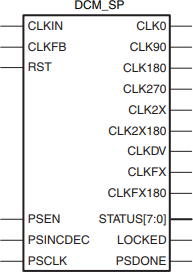
but there are also a few parameters, in particular CLKFX_MULTIPLY and CLKFX_DIVIDE
that allow to indicate the output clock with a integer ratio: in our case we need an output clock of 16MHz from the
50MHz clock of the mojo so we need to apply a factor of \({8\over 25}\).
Generally you can use Coregen to create an appropriate module with the desired clock
so to have all the value set automagically.
However, instantiating a DCM_SP is not enough, we have to route the clock signal inside
the clock network with appropriate buffers.
Buffers
The BUFG clock buffer primitive drives a single clock signal onto the clock network.
The CLKIN input of DCM_SP must belong to the clock network and indeed we get the
clock from the mojo's crystal and use the IBUFG primitive to do that.
It's not a big deal but sometimes ISE complains about clock stuffs if you generate
the clock using Coregen and use the same input signal for something else.
The second step included the adding of a multiplexer for the clock signal: a FPGA usually has dedicated resources to deal with the particular kind of signals that are the clocks; in our case we need to switch from a continous clock to a pulse one.
In order to do that I used the BUFGMUX, it has three signals: I0 and I1 for the inputs, O
for the unique output and S a signal to indicate which input to enable. Using this primitive
garantee that the input and output signal are correctly in phase.
ODDR2
There is the problem to get signals in and out of a FPGA: a lot of the job depends on which kind of signal, is it differential, what level, etc...
To manage this you have to refer to the Spartan-6 FPGA SelectIO Resources.
https://forums.xilinx.com/t5/Spartan-Family-FPGAs/how-to-instantiate-ODDR-block/td-p/232589 https://forums.xilinx.com/t5/Spartan-Family-FPGAs/How-to-use-input-clock-signal-without-DCM-PLL/td-p/233055
The final form of the top module is the following
module mojo_top(
    // 50MHz clock input
    input clk_mojo,
    // Input from reset button (active low)
    input rst_n,
    // cclk input from AVR, high when AVR is ready
    input cclk,
    // Outputs to the 8 onboard LEDs
    output[7:0]led,
    // AVR SPI connections
    output spi_miso,
    input spi_ss,
    input spi_mosi,
    input spi_sck,
    // AVR ADC channel select
    output [3:0] spi_channel,
    // Serial connections
    input avr_tx, // AVR Tx => FPGA Rx
    output avr_rx, // AVR Rx => FPGA Tx
    input avr_rx_busy, // AVR Rx buffer full
     input  btn_select_clk,
     input btn_manual_clk,
    output clk_target,
    output clk_16b,
    output clk_16c
);


wire rst = ~rst_n; // make reset active high

// these signals should be high-z when not used
assign spi_miso = 1'bz;
assign avr_rx = 1'bz;
assign spi_channel = 4'bzzzz;

reg [7:0] led_r;

assign led = led_r;

/*
 * Generates the clocks used for glitching
 */
clk_core clk(
    .clk(clk_mojo),
    .clk_16a(clk_16a),
    .clk_16b(clk_16b),
    .clk_16c(clk_16c)
);

/*
 * When click the button we toggle the active clock
 */
btn_toggle clk_selection(
    .clk(clk_16a),
    .btn(btn_select_clk),
    .out(enable_clk)
);
/*
 * Here we have the single step clock
 */
btn_clk clk_manual_module(
    .clk(clk_16a),
    .btn(btn_manual_clk),
    .pulse(clk_manual)
);

BUFGMUX clk_mux(
    .I0(clk_16a),
    .I1(clk_manual),
    .S(enable_clk),
    .O(clk_target_internal)
);
ODDR2 #(
      .DDR_ALIGNMENT("NONE"),
      .INIT(1'b0),
      .SRTYPE("SYNC")
   ) ODDR2_a (
      .Q   (clk_target), // 1-bit DDR output data
      .C0  (clk_target_internal),     // 1-bit clock input
      .C1  (~clk_target_internal),    // 1-bit clock input
      .CE  (1'b1),         // 1-bit clock enable input
      .D0  (1'b1),
      .D1  (1'b0),
      .R   (1'b0),   // 1-bit reset input
      .S   (1'b0)    // 1-bit set input
   );
endmodule
Circuit
Obviously to single step the microcontroller I need to connect it to the FPGA: at first I tried
to use a breadboard but with my huge disappointment I discovered that because of the noise
induced by the jumper wires and the breadboard itself, also without pumping the clock inside
the XTAL1 pin, the ATMega was running at like a few kHz.
To riduce parassitic signals I soldered a protoboard with only the UART, VCC, GND
and the XTAL1 pins connected externally. If you want the schematics is pratically equal
to the circuit described in this old post
To complete the device a simple keypad to control the switching from continous clock to a manual one is added.
Code
To test my device I re-adapted the simplest program for a microcontroller: the blink sketch: it simply lights a led for 5 seconds when started and then alternates between on and off without delay
/*
 * A simple sketch that blinks a led on pin A5 (port PC5)
 */
#include <avr/io.h>
#include <util/delay.h>

int main() {
    DDRC  = (1 << PC5);       //Sets the direction of the PC5 to output

    PORTC |= (1 << PC5);       //Sets PC5 high
    _delay_ms(5000);
    PORTC &= ~(1 << PC5);       //Sets PC5 low
    _delay_ms(1000);

    cli();
    while (1) {
        PORTC |= (1 << PC5);
        PORTC &= ~(1 << PC5);
    }
}
it uses directly the I/O memory port of the ATMega in order to avoid the overhead
of calling digitalWrite() that is used in normal Arduino sketches.
If you want to understand what PORTC, DDRC etc... refer to, use the
datasheet
and look for the I/O-Ports section.
To check the assembly instruction obtained compiling this code I used radare2:
$ r2 -AA -a avr fpga/mojo/GlitchGen/avr/build-uno/avr.elf
[0x00000000]> pdf @ sym.main
/ (fcn) sym.main 52
|   sym.main ();
|              ; CALL XREF from 0x00000080 (sym.main)
|           0x00000080      80e2           ldi r24, 0x20
 ; set value of I/O addr 0x07 (Port C Data Direction Register) to 0x20
|           0x00000082      87b9           out 0x07, r24
 ; set 5th bit of I/O addr 0x08 (Port C Data Register)
|           0x00000084      459a           sbi 0x08, 5
|           0x00000086      2fef           ser r18       ; r18 = 0xff
|           0x00000088      83e2           ldi r24, 0x23
|           0x0000008a      94ef           ldi r25, 0xf4
|              ; JMP XREF from 0x00000092 (sym.main)
|       .-> 0x0000008c      2150           subi r18, 0x01
|       :   0x0000008e      8040           sbci r24, 0x00
|       :   0x00000090      9040           sbci r25, 0x00
|       `=< 0x00000092      e1f7           brne 0x8c       ; loop for 0xf423 cycles
|       ,=< 0x00000094      00c0           rjmp 0x96
|       |      ; JMP XREF from 0x00000094 (sym.main)
|       `-> 0x00000096      0000           nop
|           0x00000098      4598           cbi 0x08, 5     ; clear 5th bit of I/O addr 0x08
|           0x0000009a      2fef           ser r18
|           0x0000009c      83ed           ldi r24, 0xd3
|           0x0000009e      90e3           ldi r25, 0x30
|              ; JMP XREF from 0x000000a6 (sym.main)
|       .-> 0x000000a0      2150           subi r18, 0x01
|       :   0x000000a2      8040           sbci r24, 0x00
|       :   0x000000a4      9040           sbci r25, 0x00
|       `=< 0x000000a6      e1f7           brne 0xa0       ; loop for 0x30d3 cycles
|       ,=< 0x000000a8      00c0           rjmp 0xaa
|       |      ; JMP XREF from 0x000000a8 (sym.main)
|       `-> 0x000000aa      0000           nop
\           0x000000ac      f894           cli
[0x00000000]> pdf @ fcn.000000ae
/ (fcn) fcn.000000ae 6
|   fcn.000000ae ();
|              ; JMP XREF from 0x000000b2 (fcn.000000ae)
|       .-> 0x000000ae      459a           sbi 0x08, 5
|       :   0x000000b0      4598           cbi 0x08, 5
\       `=< 0x000000b2      fdcf           rjmp 0xae
The last three instructions are what interest me; using the Instruction set cheat sheet as reference for the number of clock cycles for instruction we have the following table
| Instruction | Clock cycles |
|---|---|
| sbi | 2 |
| cbi | 2 |
| rjmp | 2 |
So if this experiment is working we should observe two steps from the led on to off and a complete loop should take six steps.
Demo
I put a simple live demo with the demostration of what is described in this post, it's a bit lagging but I think gives an idea of what's happening
The code for all this stuff is on my github, in particular at this repo and revision (something could be slighty different).
Comments
Comments powered by Disqus