Mojo FPGA development board
I have a new shiny toy, a Mojo V3 development board: it's primarly intended as FPGA
playground, but what's this FPGA you are talking about?
FPGA
Simply put, an FPGA is a technology that allows to design chip using software i.e.
a FPGA is not programmed but configured using a special kind of language, a hardware description language
(HDL). The most common
is Verilog.
Its primary scope is to design and test a chip before to start to build it for real: if you are used to design software you know that bug in production are a bad thing, but you also know that a fix can be done in order of hours and hypotetically (depending on your platform) be deployed in a time scale of a day maybe.
With hardware design this is not obviously the case: first of all who design a chip doesn't have at his disposal the machinery needed to create it, the design must be sent to a factory that after a delay of several months return to you the final product.
Any error in the real chip causes the entire process to be repeated! Take in mind that the cost of all of this is around the million dollars scale!
This video talks about the problems
in designing a chip like the x86 one.
Mojo
The mojo can be described as an arduino for FPGA: not only because has an
ATMega chip that is used to program the board.
Normally a FPGA
has appositely crafted programmer to put the configuration in them (doc
here) in
this board instead the arduino-like chip presents on it, acts as programmer
thanks to a special bootloader
burned into it: the ATMega loads the bitstream into the flash, the FPGA
when resets, loads the code from there.
An important thing to remember is that the configuration is stored temporary
on the memory of the FPGA, after a new power-up the chip needs to be
re-configured again. By the way the Mojo allows to store a resident bitstream
into the flash that is loaded using the ATMega when the board is powered.
The specs of the board are
-
Spartan 6 XC6SLX9: (Spartan-6 Family Overview) contains 9152 logic cells and 11440 flip-flops - 84 digital pins
- 8 analog pins
- package
TQG144 - speed grade -2
Pinout
The pinout is a little strange at first, here the reference for the chip with the correct pinout naming and here the complete reference.
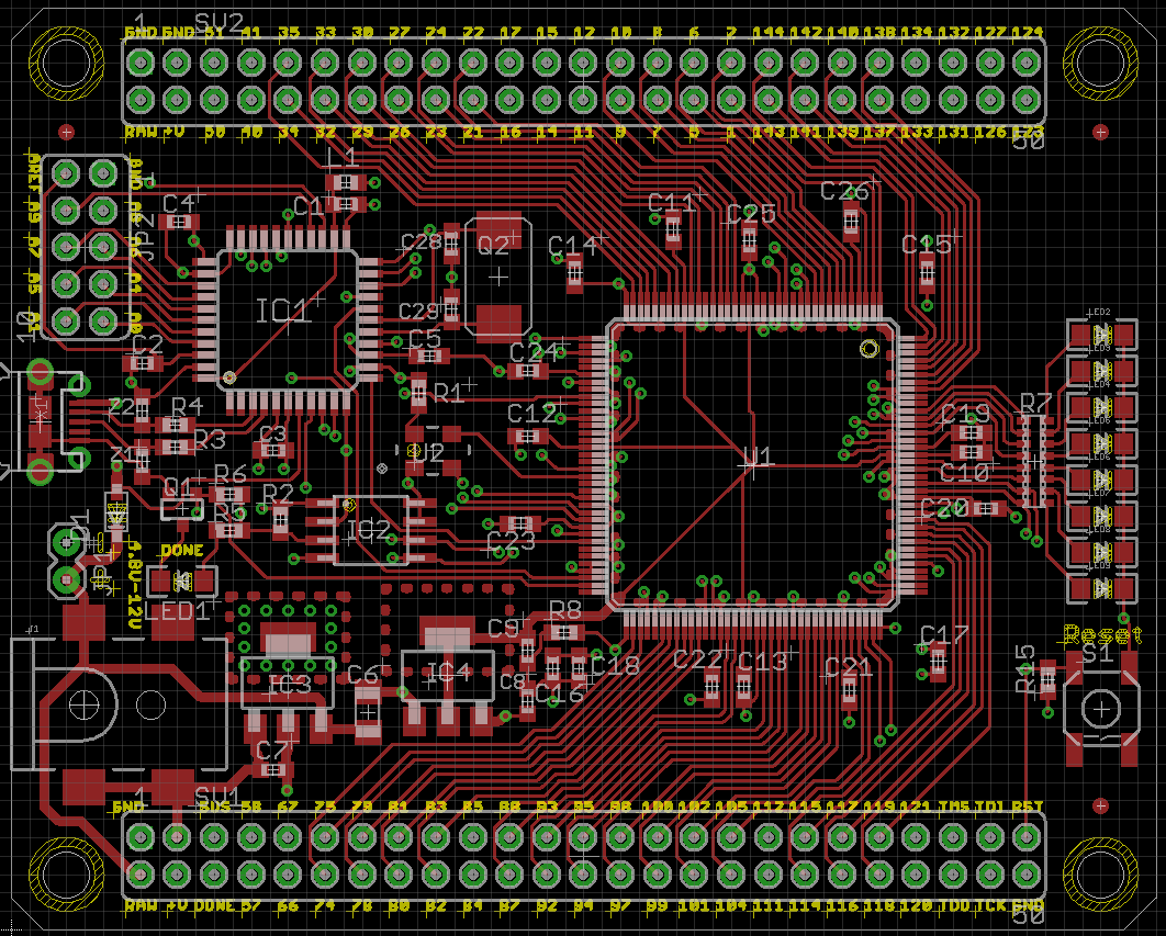
For reference I made a grab of the layout of the board:
The pins used in a design must be indicated in a file with extension ucf (stands for user constraints file) that
pratically indicate to the design which signals are exposed and where.
Like any other documentation is a big pdf.
Development environment
The bad side of writing code for this technology is that the toolsets are pratically only proprietary, with all the
programs pretty heavy (ISE occupy approximately 20GB on disk).
In order to use this board you need to install the Xilinx software named ISE, the instruction
are here.
However to start as beginner you can use the mojo ide.
Comments
Comments powered by Disqus