Implementing Text mode for a VGA controller in Verilog
After having written about implementing a VGA controller in Verilog I wanted to improve it with a new functionality: the Text mode.
The Text mode is described in an excellent way by Wikipedia
Text mode is a computer display mode in which content is internally represented
on a computer screen in terms of characters rather than individual pixels.
Typically, the screen consists of a uniform rectangular grid of character cells,
each of which contains one of the characters of a character set
It's not a difficult project but it's worth making. I start laying out the diagram of the controller:
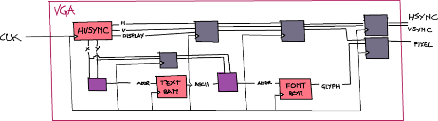
The purple boxes are combinatorial logic realizing the translation between screen's coordinates and the memories addresses, the grey boxes instead are flip-flops intended to sync signals between the different internal blocks of the module: this will be explained later.
With respect to the previous VGA controller here we have two new elements: the ROM with
the predefined glyph and the Text RAM containing the characters I want to display on
screen. These are memories.
The hvsync_generator is pratically unchanged from the version of the previous post.
Memory
A memory is a device capable of storing and accessing data (you know, memory); usually are characterized by its address width and output width.
Since I'm using a spartan-6 FPGA I have access to some primitive useful to generate memories using the Core generator (here a guide: Spartan-6 FPGA Block RAM Resources).
For the ROM I have the following diagram
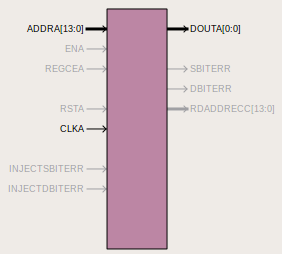
the clock (CLKA) signal is obvious, the other are the address
line (ADDRA) and the output (DOUTA); the width of these lines
are determined by the organization of the memory you need.
In my case I need the ROM to contain the data necessary to draw
the pixel of a single character: I'll use 128 ASCII characters
and each one will be represented with a 8x16 grid; in this way I
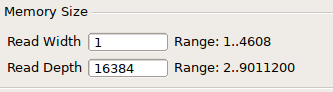
need 16384 bits. Since I want to access the bits individually I configure
the memory to be 16Kx1
Different story is the RAM: I need a read and write memory device
that will contain an ASCII character index for each one of the block
in which the screen is divided; being the size of each character be 8x16
we have, for a resolution of 640x480, 80 columns and 30 rows.
This means the we need 2400 bytes, i.e. the memory organized as 2400x8.
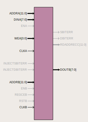
Since I need to write, there are two signal lines for that (DINA and ADDRB)
that in this implementation will remain unused.
Implementation
How we translate the screen's coordinates into text memory address and glyph memory address?
The idea here is that the value of the pixel is decided calculating in which \(column, row\) belongs: this can be determined using its coordinates \((x, y)\) with a division respectively by 8 and 16; in digital logic is simpler to take only the most significant bits of these signals:
// (column, row) = (x / 8, y / 16)
assign column = x[9:3];
assign row = y[8:4];
and at this point we can calculate the address into the text memory in order to
extract the ASCII character we need
assign text_address = column + (row * 80);

text_memory tm(
  .clka(clk), // input clka
  .wea(wea), // input [0 : 0] wea
  .addra(text_address), // input [11 : 0] addra
  .dina(dina), // input [7 : 0] dina
  .clkb(clk), // input clkb
  .addrb(text_address), // input [11 : 0] addrb
  .doutb(text_value) // output [7 : 0] doutb
);
The final value of the pixel is obtained using the modulo of the pixel's coordinates
as index for the glyph into the ROM
// here we get the remainder
always @(posedge clk) begin
    glyph_x <= x[2:0];
    glyph_y <= y[3:0];
end
                     // text_value * 128 + glyph_x + (glyph_y * 8)
assign glyph_address = (text_value << 7) + glyph_x + (glyph_y << 3);

blk_mem_gen_v7_3 glyph_rom(
  .clka(clk), // input clka
  .addra(glyph_address), // input [13 : 0] addra
  .douta(pixel[0]) // output [0 : 0] douta
);
Also here the multiplications by power of two are implemented with simpler left shifts.
Glyph and ROM
To display characters I need obviously some of them; for this project I used the
Unicode VGA font. This font
is distributed using the BDF format.
This format is, simply put, a text format that descibes the geometry and the points forming the glyph
STARTCHAR space
ENCODING 32
SWIDTH 480 0
DWIDTH 8 0
BBX 8 16 0 -4
BITMAP
00
00
00
00
00
00
00
00
00
00
00
00
00
00
00
00
ENDCHAR
In order to be used into the Xilinx IDE, the glyph must be converted into a COE
format, that is simply a binary representation of the words into the memory.
Since I didn't know any program that does that, I modified an existing program that
converts BDF glyphs into C header files and added the option to dump in the
needed format: the repo is here bdf2c but don't look
at the code, is very ugly :P.
As final step I dumped the characters needed
$ cat fpga/mojo/VGAGlyph/font/uni_vga/u_vga16.bdf | /opt/bdf2c/bdf2c -z glyph.coe -b
and synthetized with the Xilinx tools the design.
Sync
The first attempt for this controller had some issues with timing, something like the situation described here.
Roughly speaking, every memory block needs one clock cycle to output the value it's storing, since
we have two memories in series we need two clock cycles to obtain the pixel values to output on the
screen. So the pixel data and the hsync and vsync signals are out of synch causing the
character to be not aligned to the side of the screen.
Another connection that needs an explicit synchronization is the combinational logic
that translates the screen's coordinates for the glyph ROM: as just said, only after
one clock cycle the ASCII value is output from the text memory, so using directly
the glyph coordinates derived from the screen ones gives you the wrong glyph data;
this is the reason for the sequential always@(posedge clk) instruction.
I want to stress here that the approach chosen is to delay the signals out of synch in order to align it; this is accomplished using some flip flops.
When I started thinking to this problem I came up with different options in order to solve it
- pass the \(x, y\) coordinates decremented of two
- pass a clock twice as fast as the one for the
hsyncandvsync - read the character memory only once every eigth clock cycles
but thanks to a chapter of "FPGA prototyping by Verilog examples" I realized that is simpler to "slow down" the signals; it's not probably a solution for all the use cases, but this particular one, where the signal data is generated continuosly, I think is a good situation.
By the way, the implementation of the delay uses the following block of code
always@(posedge clk) begin
    hsync_delayed1 <= hsync_out_original;
    hsync_delayed2 <= hsync_delayed1;
    hsync_delayed3 <= hsync_delayed2;

    vsync_delayed1 <= vsync_out_original;
    vsync_delayed2 <= vsync_delayed1;
    vsync_delayed3 <= vsync_delayed2;

    inDisplayAreaDelayed1 <= inDisplayArea;
    inDisplayAreaDelayed2 <= inDisplayAreaDelayed1;
end

assign hsync_out = hsync_delayed3;
assign vsync_out = vsync_delayed3;
inside the VGA module.
Summary
My advice, when some issue arises from a design, is to draw explicitely a diagram of the different blocks composing your system like my awesome™ hand-drawn scheme.
In this way you can see clearly the timing and connections. The best way however is to create a reliable testbench to test the design, but this is a topic for another day.
At the end it seems to work just fine :)

If you are interested in the project, the source code can be found on github.
Comments
Comments powered by Disqus