Studying ATMega's clock
As any computing device based on transistors and flip-flop, a microcontroller needs a clock to give the "rythm" for the cpu and peripherals. In particular for the ATMega328p the clock distribution is the following
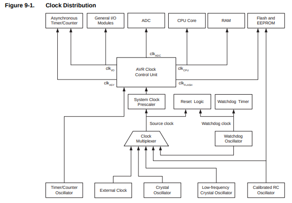
(for more information look at the datasheet).
Here I describe the ATMega328p but a lot of informations are valid for other microcontrollers of the same family and for some aspects also for any kind of microcontroller.
Available options
This device allows for different sources as clock, the selection is
done by setting the fuse bits CKSEL 3..0
Fuse CKSEL3..0
|
Note | |
|---|---|---|
| Low power cystal oscillator | 1111 - 1000 | typical configuration for an Arduino, it gives the lowest power consumption, but is not capable of driving other clock inputs, and may be more susceptible to noise in noisy environments |
| Full swing cystal oscillator | 0111 - 0110 | the crystal oscillates along the power rail, it is useful for driving other clock inputs and in noisy environments. It has high current consumption. Note that it will only operate for VCC = 2.7 - 5.5 volts |
| Low frequency cystal oscillator | 0101 - 0100 | optimized for use with a 32.768kHz watch crystal |
| Calibrated internal RC oscillator | 0010 | provides an approximate 8.0MHz clock, it's voltage and temperature dependent but can be user calibrated |
| External clock | 0000 |
Note that the CKSEL0 and SUT1..0 bits configure the startup time, i.e.
the number of stable clock cycles needed to successfully start-up the device.
Just as reminder, these are all bits from the low fuse:
| CKDIV8 | CKOUT | SUT1 | SUT0 | CKSEL3 | CKSEL2 | CKSEL1 | CKSEL0 |
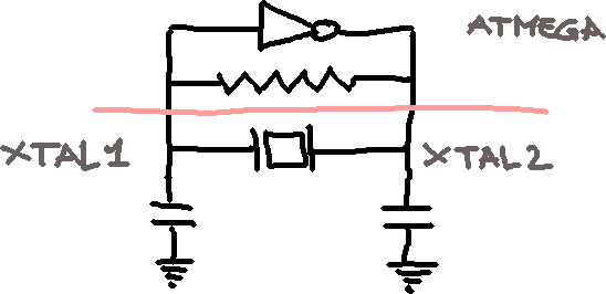
For all but internal RC oscillator the pin to use to connect the oscillator
are XTAL1 and XTAL2 (pin PB6 and PB7 respectively). They
are the input and output of an inverting amplifier which can be configured
for use as an On-chip oscillator; but what does it mean?
On-Chip oscillator
Following the Application Note 118 about CMOS Oscillators
we know that using an odd number of NOT gates we can create the following
circuit
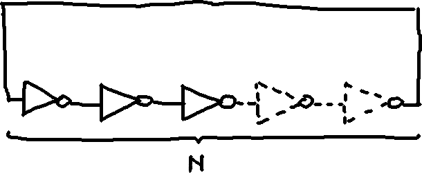
that generates a clock with frequency
$$ f = {1\over 2nT_p} $$
where \(T_p\) is the propagation delay for gate.
In the same application note is indicated the schematics for a crystal oscillator that I think is the same internal circuitery used into the ATMega for the on-chip oscillator that I imagine like this
Reading the clock signal
For a future project I want to know the electrical characteristics of the clock signal used in an arduino, but if I connect directly the probe with the pins the system stops to work probably because this process alters the capacitance of the on-chip oscillator and make this unusable. Indeed in the datasheet are indicated with precision the values of capacitance that are needed to make the crystal oscillate correctly (tipically 22pF).
To allow a probe to read a signal from the oscillator I need a buffer, i.e. a circuit
that isolate the oscillator from the probe. In my setup for
this experiment I used a BUF634 with a
+-5V as power supply and its input connected to the XTAL2 pin. Obviously the output
is connected with my oscilloscope's probe.
The signal as seen from my oscilloscope screen is
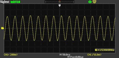
(this is dumped using the script described in another post)
At this point I can read a signal of a little less than 1 Volt (in the image above the signal
is symmetric with respect to the zero value but this happens because I use the AC coupling,
in reality is all positive).
Comments
Comments powered by Disqus